Availability: In stock
Couldn't load pickup availability
Free shipping and returns available on all orders!
We ship all orders within 5-10 business days
We advise routinely dusting your items with a gentle cleanser to preserve its look. Periodically, it may need to be softly wet with a mild detergent solution.
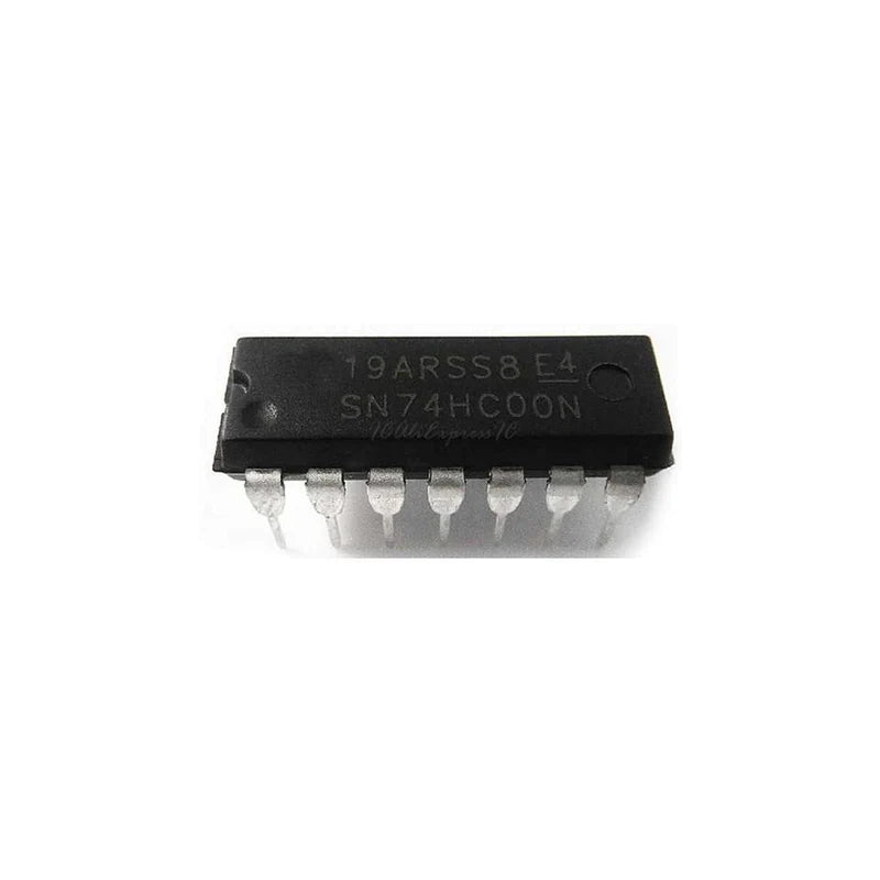
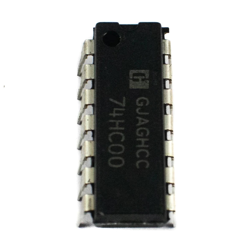
74HC series ICs are High-speed logic gates with very low power consumption that utilize advanced silicon-gate CMOS technology and 74HC00 is one of them. 74HC00 ICs contain 4 independent, 2 input NAND gate. The boolean expression can be written as Y = ( A.B )’ for each NAND gate. Internal Structure of 74HC00 device,
 The 74HC00 ICs have a wide operating range of VCC from 2 V to 6 V. Maximum current consumption is 20 uA through Icc and 1 uA per input pin. And the propagation delay is 8-9 ns. They can drive 10 LS-TTL loads at a time. This means that the single output pin of the NAND gate can drive 10 TTL-based Low-Power Schottky( LS ) input pins. They can provide 4 mA on outputs at 5 V VCC. They allow inputs and outputs up to VCC. Recommended operating VCC is 5 V. Load Current can reach up to 25 mA per output pin and 50 mA for overall pins in between 0 V to VCC.
Specification:
| Operating Voltage Range | 2.0 to 6.0 V |
| Package | DIP−14 |
| Input Current | 1 uA |
| Powering Current | 20 uA |
| Output Current at VCC | 4 mA |
| Fan-Out | 10 LS-TTL Load |
| Propagation Delay | 8 ns |
| Temperature Range | -65 °C to +150 °C |
Pin Configuration:
| Input Pins | 1, 2, 4, 5, 9, 10, 12, 13 |
| Output Pins | 3, 6, 8, 11 |
| Power Supply (VCC) | 14 |
| Ground (GND) | 7 |
Applications:


