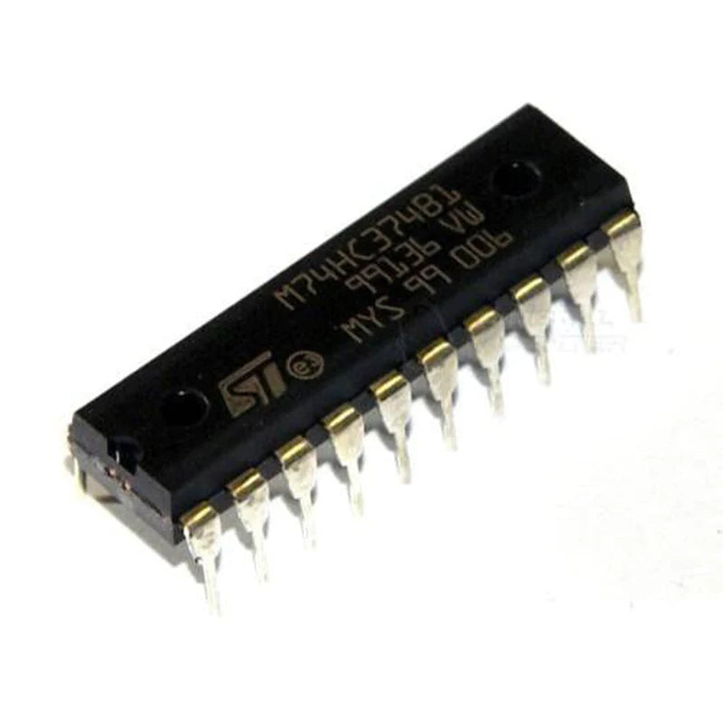
74HC series ICs are High-speed logic gates with very low power consumption that utilize advanced silicon-gate CMOS technology and 74HC374 is one of them. 74HC374 ICs contain eight positive-edge-triggered D-type flip-flops with 3-Output states i.e. High, Low, and High Impedance. Which is designed specifically for driving highly capacitive or relatively low-impedance loads. High Impedance comes to active low enable pin of these ICs where output-enable (OE)’ input places the eight outputs in either a normal logic state (high or low logic levels) or the high-impedance state. (OE)’ does not affect the internal operations of the flip-flops. Old data can be retained or new data can be entered while the outputs are in the high-impedance state.
The 74HC374 ICs have a wide operating range of VCC from 2 V to 6 V. Maximum current consumption is 80 uA through Icc and 1 uA per input pin. And the propagation delay is 14 ns. They can drive 10 LS-TTL loads at a time. Which means that the output pin of D-type flip-flop can drive 10 TTL based Low-Power Schottky( LS ) input pins. They can provide 6 mA on outputs at 5 V VCC. They allow inputs and outputs up to VCC. Recommended operating VCC is 5 V. Load Current can reach up to 35 mA per output pin and 70 mA for overall pins in between 0 V to VCC.
Specification:
| Operating Voltage Range | 2.0 to 6.0 V |
| Package | DIP−20 |
| Input Current | 1 uA |
| Powering Current | 80 uA |
| Output Current at VCC | 6 mA |
| Fan-Out | 10 LS-TTL Load |
| Propagation Delay | 14 ns |
| Temperature Range | -65 °C to +150 °C |
Pin Configuration:
| Data Input (D[0:7]) | 3, 4, 7, 8, 13, 14, 17, 18 |
| Output Pins (Q[0:7]) | 2, 5, 6, 9, 12, 15, 16, 19 |
| Active Low Enable (OE') | 1 |
| Clock (CLK) | 11 |
| Power Supply (VCC) | 20 |
| Ground (GND) | 10 |