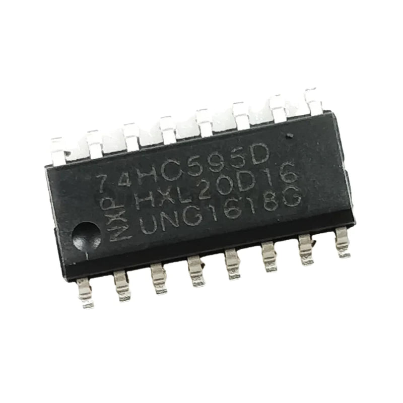
The 74HC595 are high-speed Si-gate CMOS devices and are pin-compatible with low power Schottky TTL (LSTTL). They are specified in compliance with JEDEC. The 74HC595 is an 8-stage serial shift register with a storage register and 3-state outputs. The shift register and storage register have separate clocks. Data is shifted on the positive-going transitions of the SH_CP input. The data in each register is transferred to the storage register on a positive-going transition of the ST_CP input. If both clocks are connected together, the shift register will always be one clock pulse ahead of the storage register. The shift register has a serial input (DS) and a serial standard output (Q7’) for cascading. It is also provided with asynchronous reset (active LOW) for all 8 shift register stages. The storage register has 8 parallel 3-state bus driver outputs. Data in the storage register appears at the output whenever the output enable input (OE) is LOW.
Pin Configuration

|
Pin Number |
Pin Name |
Description |
|
1,2,3,4,5,6,7 |
Output Pins (Q1 to Q7) |
parallel data output |
|
8 |
Ground |
Connected to the Ground of the circuit |
|
9 |
Q7 |
serial data output |
|
10 |
(MR) Master Reset |
master reset (active LOW) |
|
11 |
(SH_CP) Clock |
This is the clock pin to which the clock signal has to be provided from MCU/MPU |
|
12 |
(ST_CP) Latch |
The Latch pin is used to update the data to the output pins. It is active high |
|
13 |
(OE) Output Enable |
The Output Enable is used to turn off the outputs. Must be held low for normal operation |
|
14 |
(DS) Serial Data |
This is the pin to which data is sent, based on which the 8 outputs are controlled |
|
15 |
(Q0) Output |
The first output pin. |
|
16 |
Vcc |
This pin powers the IC, typically +5V is used. |
FEATURES
APPLICATIONS
|
Supply voltage |
2 - 6V |
|
TEMPERATURE RANGE |
−40°C to +125°C |
|
Pins |
16 |
|
Package |
SO16 |
|
Ambient temperature |
−40°C ~ +125°C |
|
Dimensions |
10mm x 6mm x 1.6mm |