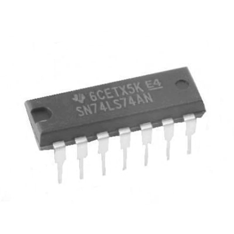
74LS Series ICs are High-Speed Logic gates, ideally a little faster than 74HC series but more power consumption is required. They are implemented with a Low-Power Schottky diode technology to achieve high switching speed. 74LS74 is one of the 74LS series IC. 74LS74 ICs contain two independent positive-edge-triggered D flip-flops with complementary outputs. These ICs can set or reset the outputs by using preset (PRE)’ or clear (CLR)’ input at a low level, regardless of the levels of the other inputs. When PRE’ and CLR’ are inactive (high), data at the data (D) input meeting the setup time requirements is transferred to the outputs on the positive-going edge of the clock pulse.
The 74LS74 ICs have an operating range of VCC from 4.5 V to 5.5 V. Maximum current consumption is 15 mA through Icc and 1 mA per input pin. And the maximum propagation delay is 25 ns. They can provide 4 mA at High Input and 8 mA at Low Input. They allow inputs and outputs up to VCC. The recommended operating VCC is 5 V.
Application:
Specification:
| Operating Voltage Range | 4.5 V to 5.5 V |
| Package | DIP−14 |
| Input Current | 1 mA |
| Powering Current | 15 mA |
| Propagation Delay | 25 ns |
| Temperature Range | -65 °C - 150 °C |
Pin Configuration:
| Input (1D, 2D) | 2, 12 |
| Inverting Output (1Q', 2Q') | 6, 8 |
| Non-Inverting (1Q, 2Q) | 5, 9 |
| Clock (1CLK, 2CLK) | 3, 11 |
| Enable Pin (ENP, ENT) | 7, 10 |
| Preset (1PRE', 2PRE') | 4, 10 |
| Power Supply (VCC) | 16 |
| Ground (GND) | 8 |