Availability: In stock
Couldn't load pickup availability
Free shipping and returns available on all orders!
We ship all orders within 5-10 business days
We advise routinely dusting your items with a gentle cleanser to preserve its look. Periodically, it may need to be softly wet with a mild detergent solution.
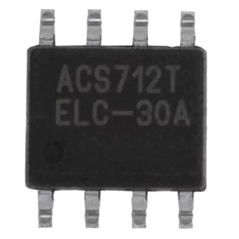
ACS712-30 consists of a precise, low-offset, linear Hall circuit with a copper conduction path located near the surface of the die. The Hall IC transforms the magnetic field created by the applied current flowing via this copper conduction route into a proportionate voltage. The magnetic signal's near proximity to the Hall transducer improves device precision. The low-offset, chopper-stabilized Bi-CMOS Hall IC, which is configured for precision after packaging, delivers a precise, proportional voltage.
When an increasing current flows along the primary copper conduction path, which is the path utilised for current sampling (from pins 1 and 2, to pins 3 and 4), the output of the device has a positive slope (>VIOUT(Q)). This conductive channel typically has an internal resistance of 1.2 mΩ, which results in minimal power loss. The gadget can survive under conditions of up to a 5-fold overcurrent thanks to the thickness of the copper conductor. The signal leads (pins 5 through 8) are electrically insulated from the terminals of the conductive path. As a result, opto-isolators or other expensive isolation methods are not necessary when using the ACS712 in applications that call for electrical isolation.
The ACS712 is provided in a small, surface mount SOIC8 package. A normal lead (Pb)-free printed circuit board assembly technique is compatible with the lead-frame's plating because it is made entirely of matte tin. Except for the flip-chip high-temperature Pb-based solder balls, which are currently exempt from RoHS, the device is Pb-free internally.
Features :-
Applications :-
| Parameter | Values |
| Model | ACS712-05 |
| Supply Voltage | 5.0 V |
| Supply current | 30 A |
| Primary Conductor Current | 1.2mOhm |
| Frequency Bandwidth | 80kHz |
| Rise Time | 5us |
| Output Capacitance Load | 10nF |
| Power-On Time | 35us |
| Optimized Accuracy Range | -20A - 20A |
| Package | SMD |


