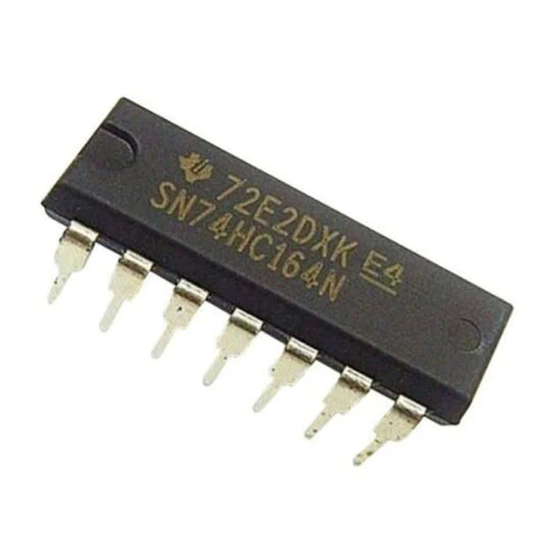
74HC series ICs are High-speed logic gates with very low power consumption that utilize advanced silicon-gate CMOS technology and 74HC164 is one of them. It has balanced propagation delay and transition times. 74HC164 ICs contain an 8-bit shift register with two input NAND gate as well as an asynchronous clear pin( CLR ). The device requires a HIGH signal at both Input A and B pins. The CLK pin of the SN74HC164 is triggered on a positive or rising-edge signal, from LOW to HIGH. Upon a positive-edge trigger, the device will store the result of the (A.B) input data line in the first register and propagate each register’s data to the next register. The data of the last register will be discarded at each clock trigger. If a low signal is applied to the CLR pin of the SN74HC164, the device will set all registers to a value of 0 immediately.
The 74HC164 ICs have a wide operating range of VCC from 2 V to 6 V. Maximum current consumption is 80 uA through Icc and 1 uA per input pin. And the propagation delay is 20 ns. They can drive 10 LS-TTL loads at a time. This means that the output pin of the shift register can drive 10 TTL based Low-Power Schottky( LS ) input pins. They can provide 6 mA on outputs at 5 V VCC. They allow inputs and outputs up to VCC. Recommended operating VCC is 5 V. Load Current can reach up to 25 mA per output pin and 50 mA for overall pins in between 0 V to VCC.
Specification:
| Operating Voltage Range | 2.0 to 6.0 V |
| Package | DIP−14 |
| Input Current | 1 uA |
| Powering Current | 80 uA |
| Output Current at VCC | 6 mA |
| Fan-Out | 10 LS-TTL Load |
| Propagation Delay | 20 ns |
| Temperature Range | -65 °C to +150 °C |
Pin Configuration:
| Data Input Pin (A, B) | 1, 2 |
| Parallel Output Pins (Q[0:7]) | 3, 4, 5, 6, 10, 11, 12, 13 |
| Active Low Clear Pin (CLR') | 9 |
| Clock Pin (CLK) | 8 |
| Power Supply (VCC) | 14 |
| Ground (GND) | 7 |
Applications: