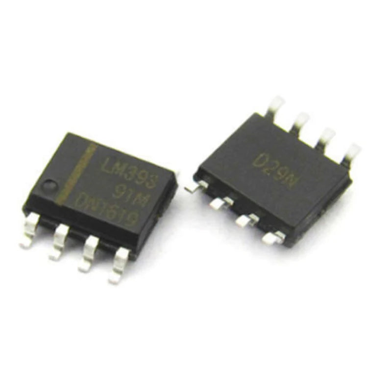
The LM393 is made up of two independent precision voltage comparators with offset voltage specifications as low as 2.0 mV max for two comparators that were especially intended to work from a single power supply over a broad variety of voltages. It is also feasible to operate from split power supplies, and the low power supply current drain is independent of the amount of the power supply voltage. These comparators also have an unusual feature in that the input common-mode voltage range includes ground, despite the fact that they are powered by a single power supply voltage. LM393 integrated circuit is the comparator version of the famous LM358 Op-Amp. The LM393 is useful since it has an open collector output that allows it to drive loads. The output transistor can drive loads up to 50V and 50mA, which is sufficient to power most TTL, MOS, and RTL loads. The transistor can also separate the load from the system ground. So, if you're seeking for a Voltage comparator to drive loads with these criteria, this IC would be a good fit.
Features
| Number of channels | 2 |
| Output type | Open Collector |
| Propagation delay time (µs) | 0.7 |
| Input V(single supply) | 2-36V |
| Input V(Dual supply) | ±1.0 ±18 V |
| Vos (offset voltage @ 25 C) (Max) (mV) | 5 |
| Iq per channel (Typ) (mA) | 0.2 |
| Input bias current (+/-) (Max) (nA) | 250 |
| Rail-to-rail | Out |
| Operating Junction temperature range | 0 to 70C |
| VICR (Max) (V) | 34.5 |
| VICR (Min) (V) | 0 |
| Dimensions | 6mm x 5mm x 1.5mm |