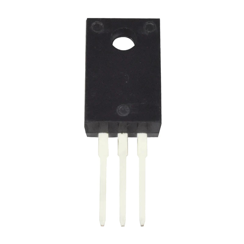


WML11N65C2 Super Junction Power MOSFET In the N layer of J-MOS, there is a P layer that is fashioned like a pillar. Alternating layers of P and N are aligned. Applying VDS causes the depletion layer to spread in the N-layer, but in SJ-MOS it does so differently than in regular D-MOS. (See illustrations of electric field intensity. The strength of the electric field reflects the condition of the depletion layer.) When it comes to D-MOS, the P/N layer contact has the strongest electric field intensity. Break-over phenomena (also known as breakdown phenomenon) occurs when the electric field intensity exceeds the limit of silicon, and this is the voltage limit. The electric field intensity in the N-layer is uniform for SJ-MOS, in contrast. As a result, an N- layer with lower resistance can be created for SJ-MOS, realizing. Its used in PC, Charger, LED TV, LCD TV Etc.
Features
Its drain to source voltage is 700V
Its used for power switching
It has lead free and halogen free construction
Low leakage current
It has the capability to improved dv/dT
| Model | WML11N65C2 |
| Type | MOSFET |
| Package | TO-220F |
| VDS | 700V |
| Max reverse operating Voltage | 650V |
| Resistance | 0.47Ohm |
| No of pins | 3 |
| Operating and Storage Temperature Range | -55°C TO 150°C |